
SYLLABUS
GS-I Prelims: Current events of national and international importance.
GS-3: Science and Technology- Developments and their Applications and Effects in Everyday Life; Indigenization of Technology and Developing New Technology.
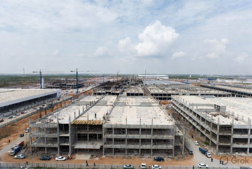
Context: The Government of India has notified a Special Economic Zone (SEZ) by Tata Semiconductor Manufacturing Private Limited at Dholera to establish the country’s first semiconductor chip fabrication plant.
Key Features of the Semiconductor Fab Project
- The SEZ will be developed over 66.166 hectareswith a proposed investment of ₹91,000 crore.
- This is India’s first chip fabrication plant.
- The SEZ is designed to support electronic hardware, software, and IT/ITES services with integrated infrastructure.
- It includes a dedicated approval and logistics mechanism to ensure ease of doing business.
- The approval was granted by the Board of Approval (BoA), the apex body for SEZ-related decisions.
- It is part of a broader push under initiatives like the India Semiconductor Mission 2.0, aimed at building a full-stack semiconductor ecosystem.
- Policy & Regulatory Reforms: Amendments to Special Economic Zones Rules, 2006 (June 2025) tailored for semiconductor manufacturing. Key reforms include:
- Reduction in minimum land requirement (50 → 10 hectares)
- Relaxation of encumbrance norms
- Inclusion of free-of-cost supplies in Net Foreign Exchange (NFE)
- Allowing Domestic Tariff Area (DTA) sales on payment of duties
- These reforms aim to promote high-value, capital-intensive investments and improve ease of doing business.
Other Approved Semiconductor & Electronics SEZs
- Micron Semiconductor Technology India Pvt Ltd is setting up a ₹13,000 crore ATMP unit in Sanand, Gujarat, to strengthen chip packaging capabilities.
- Hubballi Durable Goods Cluster Private Limited is establishing an electronics components manufacturing SEZ in Dharwad, Karnataka.
- CG Semi Pvt Ltd is developing a ₹2,150 crore OSAT facility to support semiconductor assembly and testing.
- Kaynes Semicon Pvt Ltd is setting up a ₹681 crore OSAT unit to enhance domestic semiconductor value chains.
Significance of the Plant
- Strengthening Semiconductor Supply Chains: With the global semiconductor market exceeding USD 600 billionand projected to cross USD 1 trillion by 2030, India’s entry into chip fabrication enhances supply chain resilience and reduces external vulnerabilities.
- Boost to Electronics Manufacturing: As India’s electronics production has already crossed USD 115 billion (2023–24), domestic chip manufacturing will support key sectors like smartphones, automobiles, and consumer electronics, reducing reliance on imports.
- Employment and Skill Development: The project will generate high-skilled jobs (~21,000)and promote advanced R&D, specialised training, and industry-academia collaboration in semiconductor technologies.
- Integration into Global Value Chains (GVCs): The fab, along with ATMP/OSAT units (like Micron Semiconductor Technology India Pvt Ltd), positions India as a reliable node in global semiconductor supply chains, complementing hubs in East Asia and the US.
- Support for Emerging Technologies: Domestic semiconductor capability is critical for AI, electric vehicles, telecom (5G/6G), defence systems, and data centres, making it strategically vital for future industries.
- Strategic & Technological Sovereignty: Indigenous chip manufacturing reduces import dependence, enhances national security, and ensures control over critical digital infrastructure.
- Catalyst for Ecosystem Development: The plant will anchor integrated semiconductor clusters, linking fabrication, design, packaging, and component manufacturing—thereby accelerating India’s transition to a full-stack semiconductor ecosystem.
About the India Semiconductor Mission
- It was launched in 2021 under the Semicon India Programme with a financial outlay of ₹76,000 crore to build a comprehensive semiconductor and display ecosystem.
- Core Objectives:
- Fabrication & Manufacturing: Promote the establishment of semiconductor fabs, ATMP/OSAT units, and display manufacturing facilities.
- Design & Innovation: Develop chip design capabilities, support semiconductor start-ups, and strengthen domestic intellectual property.
- Research & Development: Encourage advanced R&D in areas like automotive electronics, telecom, and next-generation chips.
- Global Partnerships: Foster international collaborations to integrate India into global semiconductor value chains.
- Key Features:
- Provides financial incentives, infrastructure support, and policy facilitation to attract global and domestic players.
- Promotes industry–academia collaboration for skill development and innovation.
- Focuses on building a complete value chain, from design to manufacturing and packaging.
- Recent Expansion (ISM 2.0 – Budget 2026): Expands beyond fabrication to include chip packaging, compound semiconductors, materials, and supply chain infrastructure.
- Aims to create a full-stack, self-reliant semiconductor ecosystem in India.