
SYLLABUS
GS-3: Science and Technology- Developments and their Applications and Effects in Everyday Life; Indigenization of Technology and Developing New Technology.
Context: The Union Cabinet has approved Semicon 2.0 with a total outlay of ₹1,27,500 crore to strengthen India’s semiconductor design and manufacturing ecosystem and provide long-term policy support to the sector.
More on the News
- Semicon 2.0 marks the next phase of the India Semiconductor Mission (ISM), expanding support from chip fabrication to the entire semiconductor value chain, including design, materials, equipment, R&D, and talent development.
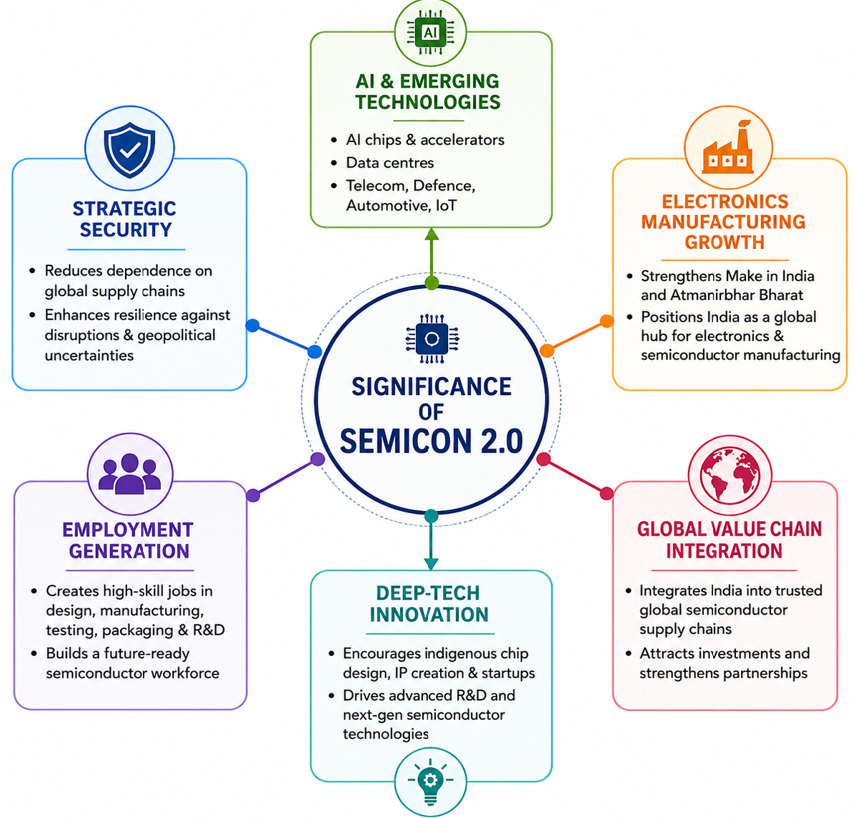
- The programme aims to position India as a trusted partner in global semiconductor supply chains amid rising demand driven by AI, electronics, telecommunications, automotive systems, defence technologies, and advanced computing.
- The approval builds on the achievements of Semicon 1.0, under which multiple semiconductor manufacturing, packaging, and design projects have been approved, and several have already commenced production.
Key Highlights of Semicon 2.0
- Semicon 2.0 is aimed to holistically build the semiconductor ecosystem on the following six pillars:
- Pillar 1: Design
- Strengthens India’s semiconductor design ecosystem by supporting chip design, semiconductor IP creation, and fabless startups.
- Builds on the momentum of over 105 startups that have already begun developing semiconductor chips in India.
- Pillar 2: Machines and Materials
- Promotes domestic manufacturing and R&D of semiconductor equipment, specialty materials, chemicals, gases, and wafers.
- Seeks to reduce import dependence and create a resilient upstream semiconductor supply chain.
- Pillar 3: Setting Up More Fabs
- Encourages establishment of additional semiconductor manufacturing facilities across the value chain.
- Covers Silicon CMOS Fabs, Compound Semiconductor Fabs, Display Fabs, and Discrete Semiconductor Fabs.
- The first semiconductor fab approved under the programme is expected to be commissioned by 2028.
- Pillar 4: Strengthening the ATMP/OSAT Ecosystem
- Expands India’s capabilities in Assembly, Testing, Marking and Packaging (ATMP) and Outsourced Semiconductor Assembly and Test (OSAT) operations.
- Aims to establish India as a major global destination for semiconductor packaging and testing services.
- Pillar 5: Research & Development (R&D)
- Supports development of next-generation semiconductor technologies beyond the current 28 nm–110 nm node capabilities.
- Encourages collaboration among industry, academia, startups, and global research institutions.
- Pillar 6: Talent Development
- Focuses on creating a future-ready semiconductor workforce through specialised education, skilling, training, and industry-academia partnerships.
- Seeks to meet the growing demand for engineers, researchers, and technicians across the semiconductor ecosystem.
Achievements Under Semicon 1.0
- Manufacturing Ecosystem Expansion: 12 semiconductor projects approved with investments exceeding ₹1.5 lakh crore, laying the foundation for India’s semiconductor manufacturing ecosystem.
- Production Commences: Facilities promoted by Micron, Kaynes, and CG Semi have begun commercial production, marking the transition from approvals to manufacturing.
- Growth of Design Ecosystem: 24 chip-design projects supported and 105 startups/MSMEs enabled with advanced EDA tools to strengthen indigenous semiconductor design capabilities.
- Rising Global Confidence: Participation of leading domestic and international companies reflects growing investor confidence in India’s semiconductor ambitions and policy framework.
Challenges in Building India’s Semiconductor Ecosystem
- Capital-Intensive Industry: Semiconductor fabrication requires massive investments, long gestation periods, and continuous technology upgrades.
- Technology Dependence: Advanced semiconductor manufacturing technologies remain concentrated among a few countries and firms.
- Ecosystem Gaps: India continues to depend significantly on imports for semiconductor-grade materials, equipment, and manufacturing inputs.
- Skilled Workforce Constraints: Sustained growth requires a large pool of specialised semiconductor engineers, technicians, and researchers.
- Global Competition: India faces intense competition from established semiconductor hubs such as Taiwan, South Korea, the United States, China, and Japan.
Way Forward
- Strengthen Semiconductor Design and IP: Expand support for indigenous chip design, semiconductor IP creation, and fabless startups.
- Develop Domestic Machines and Materials Ecosystem: Build capabilities in semiconductor equipment, chemicals, gases, wafers, and specialty materials.
- Accelerate Fabs and ATMP/OSAT Facilities: Ensure timely commissioning of approved manufacturing and packaging projects.
- Invest in Advanced R&D: Develop next-generation semiconductor technologies through stronger industry-academia collaboration.
- Expand Talent Development: Scale up semiconductor-focused education, skilling, and research programmes to meet future workforce requirements.
- Deepen Global Integration: Position India as a trusted semiconductor partner by integrating more deeply into global value chains and attracting strategic investments.