
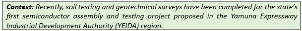
- Uttar Pradesh is set to launch its first semiconductor assembling and testing project in the Yamuna Expressway Industrial Development Authority (YEIDA) area.
- The soil testing and geo-technical survey for the project have been completed, and a bhoom is expected to take place in mid-January.
- The project is being viewed as a key milestone under the “Developed Uttar Pradesh 2047” roadmap.
About the Project
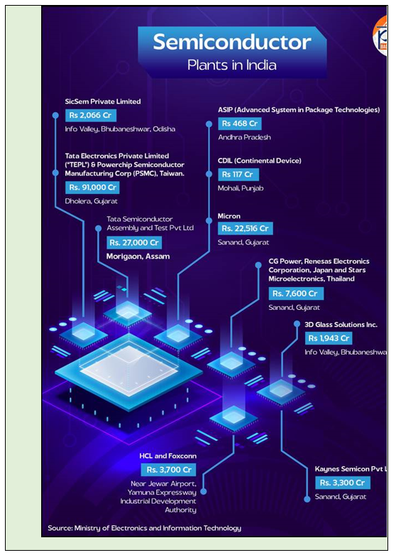
- It is being developed by Vama Sundari Investments, a joint venture between HCL and Taiwan’s Foxconn.
- Land Allocation and Investment: 48 acres of land is allocated for the project, with a proposed investment of ₹3,706 crore.
- Manufacturing Focus: The project will involve the development of display driver chips and power management chips used in mobile and electronic devices.
- Significance: It will provide a strong foundation for a three-tier model of investment, employment, and innovation, while also connecting the state to a global network of high-tech industries.
- The project is expected to create approximately 3,780 employment opportunities.
- Incentives granted under Semiconductor policy 2024: The project has been granted a 75% discount on land costs, a 100% waiver on stamp duty and registration charges, and access to water and power banking for uninterrupted operations.