
SYLLABUS
GS-3: Indian Economy and issues relating to planning, mobilization of resources, growth, development and employment.
Context: The Ministry of Electronics and Information Technology has sanctioned 24 chip design projects under the Design Linked Incentive Scheme to strengthen India’s fabless semiconductor ecosystem and reduce import dependence.
More on the News
- The initiative is part of the larger Semicon India Programme implemented through the India Semiconductor Mission.
- The Union Cabinet had approved the comprehensive Semicon India programme with a financial outlay of INR 76,000 crore for the development of a sustainable semiconductor and display ecosystem in 2021.
- These projects cover strategic areas such as video surveillance, drone detection, energy meters, microprocessors, satellite communications, and broadband and IoT Systems-on-Chip.
- The approvals aim to strengthen India’s domestic semiconductor design capability and help firms move up the semiconductor value chain.
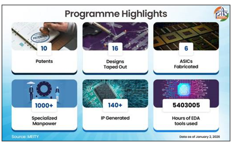
- DLI-supported projects are scaling rapidly, with 16 tape-outs, 6 ASIC chips, 10 patents, 1,000+ engineers engaged, and over 3× private investment having been leveraged.
- Alongside DLI, the Chips to Startup Programme is being implemented to generate about 85,000 industry-ready manpower in chip design at undergraduate, postgraduate, and doctoral levels.
Importance of Semiconductor Design
- Semiconductor chip contributing up to 50% of value addition, 20–50% of Bill of Materials cost (BOM), and 30–35% of global semiconductor sales via the fabless segment.
- The absence of strong fabless capability forces countries to depend on imported core technologies even when electronics are manufactured locally.
- Building a robust fabless ecosystem enables ownership of intellectual property and strengthens long-term technological leadership.
About Design Linked Incentive (DLI) Scheme
- Nodal Ministry: The scheme, launched in December 2021 by the Ministry of Electronics and Information Technology (MeitY).
- Objectives:
- The scheme aims to offset structural disadvantages faced by India’s domestic semiconductor design industry.
- It seeks to promote indigenous chip design and reduce reliance on imported semiconductor intellectual property.
- It focuses on nurturing startups and MSMEs to build a globally competitive fabless ecosystem.
- Eligibility: Startups, MSMEs, and domestic companies owned by resident Indian citizens are eligible beneficiaries.
- Coverage: The scheme supports the entire lifecycle of semiconductor design from development to deployment, covering integrated circuits, chipsets, systems-on-chip, systems, and intellectual property cores.
- Incentives: The scheme provides reimbursement of up to 50 percent of eligible design expenditure subject to a specified cap. It also offers deployment-linked incentives based on net sales for a fixed period.
- Infrastructure Support: The ChipIN Centre provides access to advanced electronic design automation tools, IP core repositories, and prototyping support. The scheme also supports post-silicon validation and testing of fabricated chips.
Achievements under the DLI Scheme
- The scheme has enabled multiple chip design tape-outs and the successful fabrication of indigenous chips.
- It has supported the filing of patents and creation of reusable semiconductor intellectual property cores.
- It has trained and engaged a large pool of specialised engineers across startups and academic institutions.
- It has leveraged significant private investment alongside government support.