
SYLLABUS
GS-3: Awareness in the fields of IT, Space, Computers, robotics, nano-technology, bio-technology and issues relating to intellectual property rights.
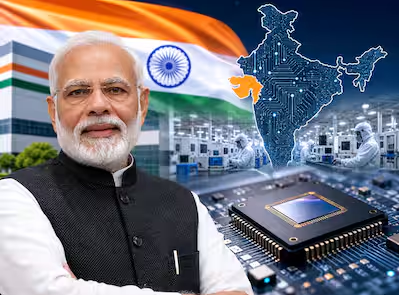
Context: The Union Cabinet approved two new semiconductor projects under the India Semiconductor Mission (ISM), including India’s first commercial Mini/Micro-LED display facility based on Gallium Nitride (GaN) technology and a semiconductor packaging facility in Gujarat.
About the Projects
• Crystal Matrix Limited (CML) Project: Crystal Matrix Limited will establish an integrated facility for compound semiconductor fabrication and ATMP (Assembly, Testing, Marking and Packaging) at Dholera, Gujarat.
- The project involves a cumulative investment of about ₹3,068 crore.
- The facility will manufacture Mini/Micro-LED display modules based on Gallium Nitride (GaN) technology and provide GaN foundry services, including epitaxy on 6-inch wafers.
- The facility will produce 72,000 sq. metres of Mini/Micro-LED display panels annually and 24,000 sets of RGB GaN epitaxy wafers annually.
- The products will be used in large displays for TVs and commercial signage, medium-sized displays for tablets, smartphones, and in-car systems, and micro-displays for XR glasses and smartwatches.
• Suchi Semicon Private Limited (SSPL) Project: Suchi Semicon Private Limited will establish an Outsourced Semiconductor Assembly and Test (OSAT) facility in Surat, Gujarat.
- The project involves an investment of around ₹868 crore.
- The facility will manufacture discrete semiconductors and focus on lead frame and wirebond packaging technologies.
- The facility will have a total production capacity of 1,033.20 million chips per annum, including 673 million SOIC (Small Outline Integrated Circuit) units and 263 million Transistor Outline (TO) units annually.
- The semiconductors will be used in power electronics, Analog Integrated Circuits (ICs), industrial systems, automotive electronics, industrial automation, consumer electronics, EV battery management systems and solar inverters.
- The two projects together are expected to generate employment for around 2,230 skilled professionals, while the SSPL project alone is expected to create around 630 direct jobs.
Significance of the Projects
• Strengthening India’s Semiconductor Ecosystem: With these approvals, the total number of projects approved under ISM has increased to 12 projects with cumulative investments of around ₹1.64 lakh crore, strengthening India’s semiconductor manufacturing capabilities across fabrication, packaging and display technologies.
• India’s First Commercial Display Facility: The CML project marks the establishment of India’s first commercial Mini/Micro-LED display manufacturing facility, reducing dependence on imports in advanced display technologies.
• Boost to Emerging Technologies: The projects will support future technologies such as Extended Reality (XR), smart wearables, automotive electronics, industrial automation and Artificial Intelligence-enabled devices.
• Supply Chain Resilience and Strategic Importance: Semiconductor manufacturing is critical for national security, digital infrastructure, and industrial competitiveness, and the projects align with the vision of Aatmanirbhar Bharat and “Make in India, Make for the World.”
• Expanding Design and Manufacturing Base: India’s growing semiconductor ecosystem is being supported through design infrastructure assistance to 315 academic institutions and 104 start-ups, while two approved semiconductor projects have already started commercial shipments and two more are expected to begin shipments soon.
About India Semiconductor Mission (ISM)
• The India Semiconductor Mission (ISM) was launched in 2021 with an outlay of ₹76,000 crore.
• It aims to build a full-stack semiconductor ecosystem in India covering:
- Semiconductor fabrication (fabs).
- Compound semiconductors.
- Semiconductor packaging and testing.
- Display manufacturing.
- Chip design and innovation.
• The scheme provides up to 50% fiscal support for eligible semiconductor and display manufacturing projects.
• Key Features of ISM 1.0:
- Focused on attracting semiconductor fabrication and packaging infrastructure.
- Encouraged domestic chip manufacturing and assembly capabilities.
- Supported semiconductor design ecosystem and start-ups.
About India Semiconductor Mission (ISM 2.0)
• Announced in the Union Budget 2026–27 with a provision of ₹1,000 crore for FY 2026–27.
• ISM 2.0 will focus on:
- Semiconductor equipment and materials manufacturing.
- Indigenous semiconductor Intellectual Property (IP).
- Advanced technology nodes such as 3 nm and 2 nm chips.
- Strengthening domestic and global semiconductor supply chains.
- Industry-led research and skill development centres.
• Sectoral Outlook:
- India’s semiconductor market was estimated at $38 billion in 2023 and is projected to reach $100–110 billion by 2030.
- By 2029, India aims to design and manufacture chips required for nearly 70–75% of domestic demand.
- By 2035, India aims to emerge among the leading semiconductor nations globally.
Sources:
PIB
PIB
Indian Express
Economictime